





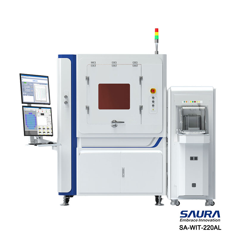

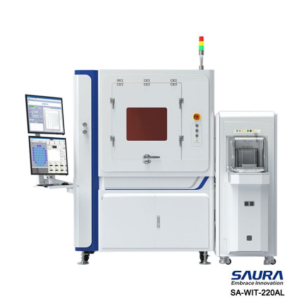
SA-WIT-220AL Fully Automatic Photonics Wafer Test System is engineered prioritizing stability, electrical noise suppression and spatial confidence, equipped with a high-precision motion control system and a premium vibration isolation system. Integrated with proprietary image processing algorithms, it enables highly stable optical characterization of small-mode-field chips and high-accuracy electrical performance measurements. Supporting fully automated wafer-scale measurement via either grating coupling or end-face coupling, the system satisfies rigorous optical test specifications and pA-level electrical signal measurement requirements. By facilitating early-stage defective chip screening at the wafer level, it prevents downstream process contamination, significantly reducing overall packaging and testing costs while enhancing production efficiency.The system has been deployed in mass production lines across domestic and international client facilities.
|
Feature |
Application |
|---|---|
|
|


Reviews
Clear filtersThere are no reviews yet.