





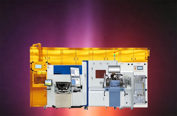
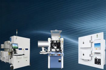

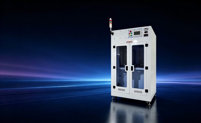
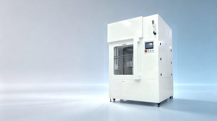
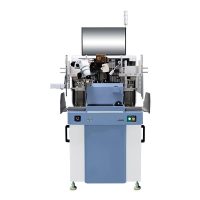
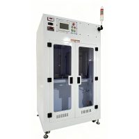


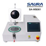
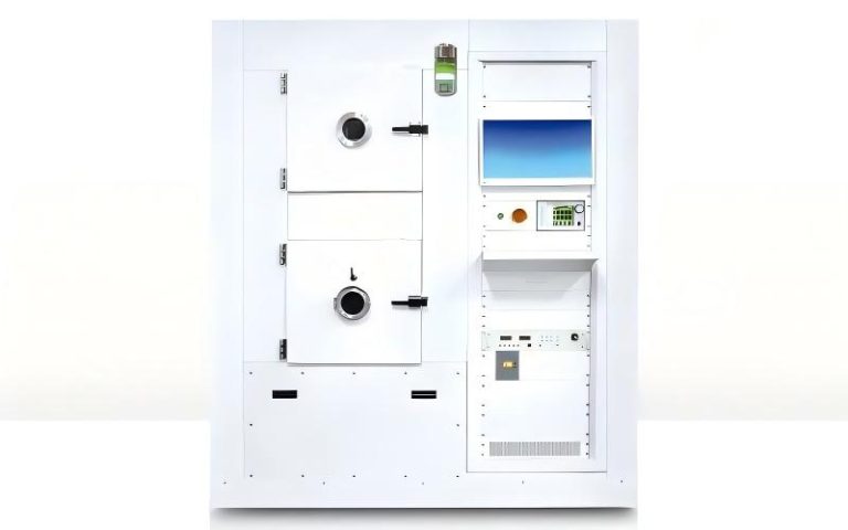
Vacuum Die Bonder SA-WB061
In stock
SKU:
SA-WB061
| Wafer Size | 150mm, 200mm, 300mm |
|---|---|
| Functions | Timing, pressurization, heating(included), vacuum(included), cooling(included) |
| Bond Pressure | 0~3bar (adjustable) |
| Throughput | Depends on the process |
| Chamber Environment | Vacuum Pump included |
| Power Requirements | 220V, 10A |
| Equipment Power | 1KW |
| Size(L×W×H)or(D×W×H) | 650mm×600mm×350mm |
| Weight | 50kg |
| Temperature Range | RT~200℃ |
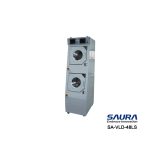



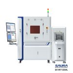
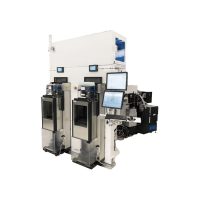
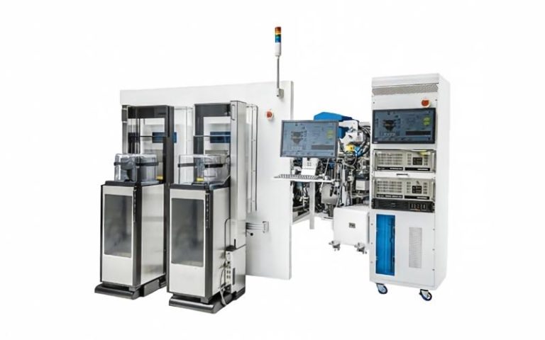
Fully Automatic Photonics Wafer Test System SA-WIT-220AL
In stock
SKU:
SA-WIT-220AL
| Wafer Size | 2″~12″ |
|---|---|
| Loading Method | Automatic |
| Loading Type | Cassette/FOUP |
| Testing Capacity | 25~50 pcs/run |
| Wafer-ID | OCR-based automatic Wafer-ID recognition with Wafer Map generation |
| Auxiliary Chuck | Enables automatic probe cleaning, RF calibration, FA calibration, PD power/polarization calibration |
| Single-Probe Marking | Yes |
| Self-Cleaning | Yes (for wafer, Chuck, probes, FA) |
| Real-Time Height Sensing | Yes |
| Chuck Height Calibration | Yes |
| Chuck Positioning Accuracy | ±2µm |
| Temperature Range | -40~125℃ |


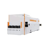
Vertical Furnace SA-Flouris X201H/P
In stock
SKU:
SA-Flouris X201H/P
| Wafer Size | 6″, 8″ |
|---|---|
| Process | FOX/STI Anneal/Pad-Oxide/Gate Oxide/BPSG Reflow/Final Alloy/Cu Anneal/N2 Anneal/Polyimide Cure |
| Compatible Materials | GaN, Si, SiC |
| Teamperature Control Accuracy | ≤±1℃ |
| Flat Zone Length | 860mm |
| Batch Size | 150/125 |
| SMIF/Open Cassette/OHT | Option |
| N2 Load Lock | Option |
| AGC | Option |
| Particle Control | ≤20@0.16μm |
| Uniformity(WIW/WTW/LTL) | ≤2%/1.5%/1.5% |
| Metal Contamination (ICP-MS/TXRF) | 5E10 |
| Loccalization Progress | Continuous improvement |
| Size(L×W×H)or(D×W×H) | 4093mm×900mm×3302mm, 4420mm×900mm×3302mm |

Advanced PVD Coating Technology: Redefine Surface Performance for Modern Industries
In the era of high-precision manufacturing and premium product upgrading, surface treatment technology has become a core factor determining product durability, aesthetics and functional stability. Physical Vapor Deposition (PVD), as an advanced vacuum thin-film coating technology, has gradually become the preferred surface enhancement solution for global high-end industries, relying on its pure physical deposition mechanism and superior coating performance. Different from traditional coating and chemical deposition processes, PVD achieves surface modification through precise physical phase transformation, bringing unprecedented comprehensive benefits to various substrates.
The Full Workflow of Modern Chip Processing Technology
Modern semiconductor chip manufacturing is a highly sophisticated, ultra-precise industrial system that integr...


AUO Showcases Micro LED Optical Communication and Glass Core Substrates Technologies at SEMICON Taiwan 2026
As AI applications continue to proliferate, demand for high-performance computing and high-speed data transmission is accelerating, making AI infrastructure capacity a critical enabler of industry growth. Targeting key technologies at the forefront of AI infrastructure, AUO will showcase its latest advancements in optical communications and advanced semiconductor packaging at SEMICON Taiwan 2026, taking place September 2-4.

Primemas at FMS 2026: CXL Full-Stack Products and Micron Collaboration on the Abaco Project
Primemas Inc. showcased its latest CXL memory innovations at the Future of Memory and Storage (FMS) 2026. At the event, the company highlighted the industry’s most comprehensive CXL memory portfolio and its strategic collaboration with Micron on the Abaco Project, a rack-scale compute system with over 100TB of CXL-attached shared and pooled memory developed for the Department of Energy’s Pacific Northwest National Laboratory (PNNL) to power next-generation, large-scale scientific AI, HPC and data-intensive workloads. The Abaco Project is supported by DOE’s Office of Science, Advanced Scientific Computing Research program.
Agentrys Raises $24.5 Million to Build Agentic Design Automation for Chipmakers
Agentrys, a startup focused on automating and continuously improving chip design, today announced that it has raised $24.5 million in funding. The total comprises an oversubscribed $19.1 million seed round led by Etna Labs, following a $5.4 million pre-seed led by MediaTek, the company’s first strategic backer. The new funding will go toward recruiting, agent-native tooling, and expanding customer engagements across verification and physical design.
MetaOptics and Elsoft Partner to Scale Next-Generation Semiconductor Optics Manufacturing Equipment
MetaOptics Ltd and Elsoft Research Berhad today jointly announced a strategic partnership to co-develop and mass produce the next generation of 12-inch large format precision, high speed metalens laser writers and leading-edge automatic testers that could sort metalens across widely applied wavelengths from visible light 425 ~ 630nm, in-frared 740 ~ 940nm and 1245 ~ 1310nm.