Substrate Preparation, Fabrication, Packaging, Supply Systems, Testing

The Full Workflow of Modern Chip Processing Technology

Modern semiconductor chip manufacturing is a highly sophisticated, ultra-precise industrial system that integrates micro-nano processing, precision testing and intelligent supply control. Every functional chip undergoes a complete standardized process chain, covering substrate preparation, wafer fabrication, packaging, performance testing and supporting supply system operation. Each link relies on professional dedicated equipment to ensure ultra-high yield and stable performance of finished products.

1. Substrate Preparation

Wafer Surface Purification & Optimization
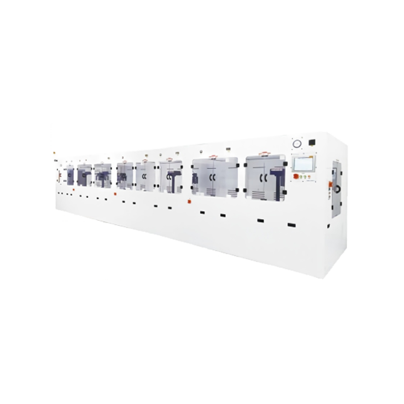
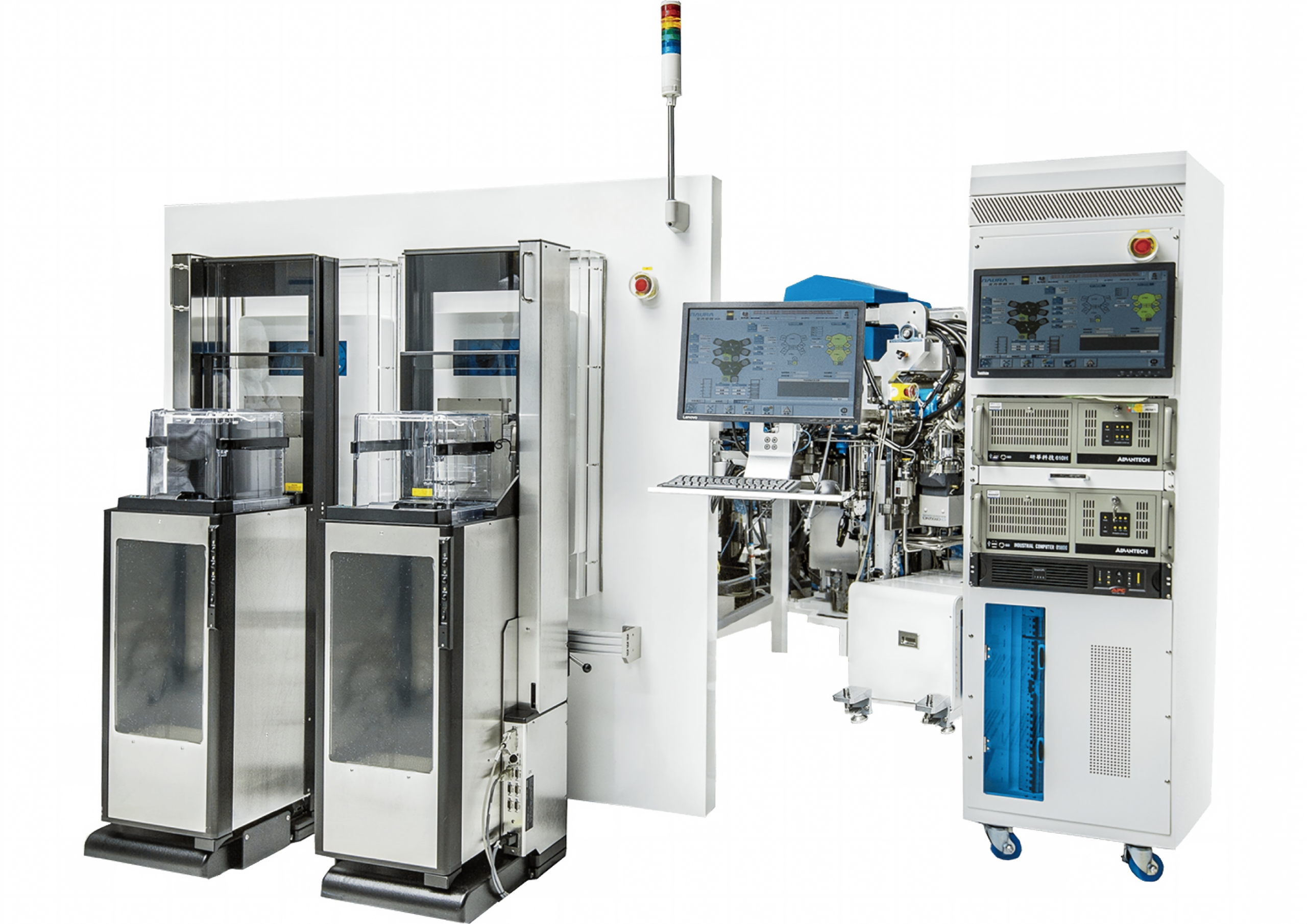
As the foundational stage of chip manufacturing, substrate preparation focuses on purifying and optimizing wafer substrates to create a flawless foundation for subsequent circuit fabrication. Surface contamination, particle residues and oxide layers are the core threats to chip quality in this stage. Professional cleaning machines are widely adopted here to conduct multi-step precision cleaning, removing micro impurities and organic contaminants on the substrate surface. Strict surface treatment and dehydration processes are implemented after cleaning to guarantee flatness, cleanliness and chemical stability of the substrate, laying a prerequisite for accurate film growth and circuit patterning.
  • Specification

Wafer Size:

4"/5"/6"/8"/12"

4"~8" Cleaning Capacity:Ā 

25pieces2baskets/batch

12"Cleaning Capacity:

25pieces/batch

Control Part:

PLC and HMI

2. Wafer Fabrication

Micro-nano Circuit Structure Construction
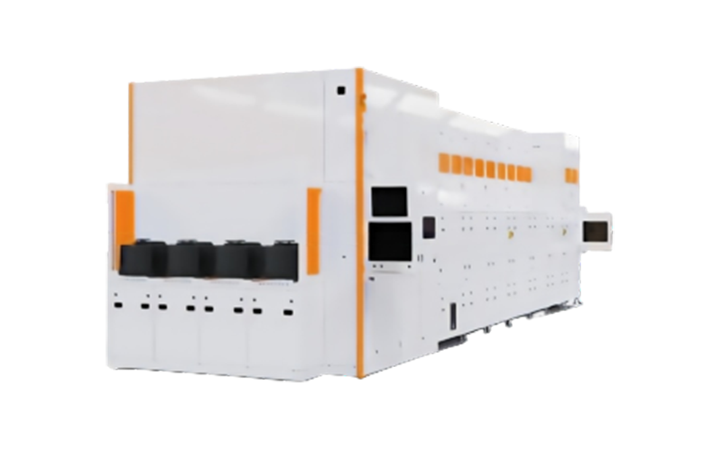
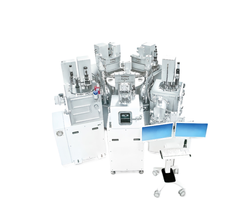
Fabrication is the core front-end process of chip formation, realizing the construction of microscopic circuit structures on qualified substrates through repeated deposition, etching and patterning cycles. Two core film-forming devices dominate the thin-film manufacturing process: CVD (Chemical Vapor Deposition) and PVD (Physical Vapor Deposition). They deposit uniform, high-purity dielectric and metal films on the substrate surface to form circuit conductive layers and insulating layers. Meanwhile, etchers perform precise micro-nano etching according to circuit design layouts, stripping redundant film materials to carve out complete circuit patterns. This cyclic processing builds multi-layer microscopic circuit networks on the wafer, forming the core functional structure of uncut chip dies.

3. Precision Packaging

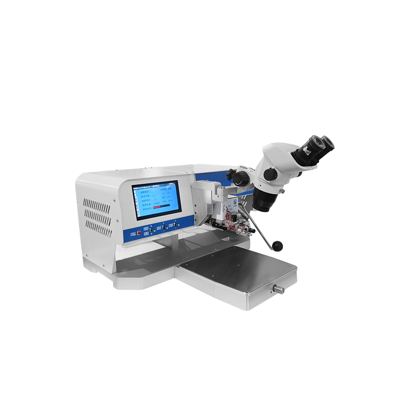
After wafer fabrication, qualified chip dies enter the packaging stage, which aims to protect delicate internal circuits, realize electrical connection and adapt to terminal assembly scenarios. As key packaging equipment, wire bondersĀ complete high-precision wire bonding between chip dies and external pins, establishing stable electrical signal transmission channels. The whole process isolates core chip components from external moisture, dust and mechanical damage through packaging materials and structural design, while optimizing heat dissipation and structural stability, turning bare dies into structurally complete and practically usable chip components.

4. Professional Testing

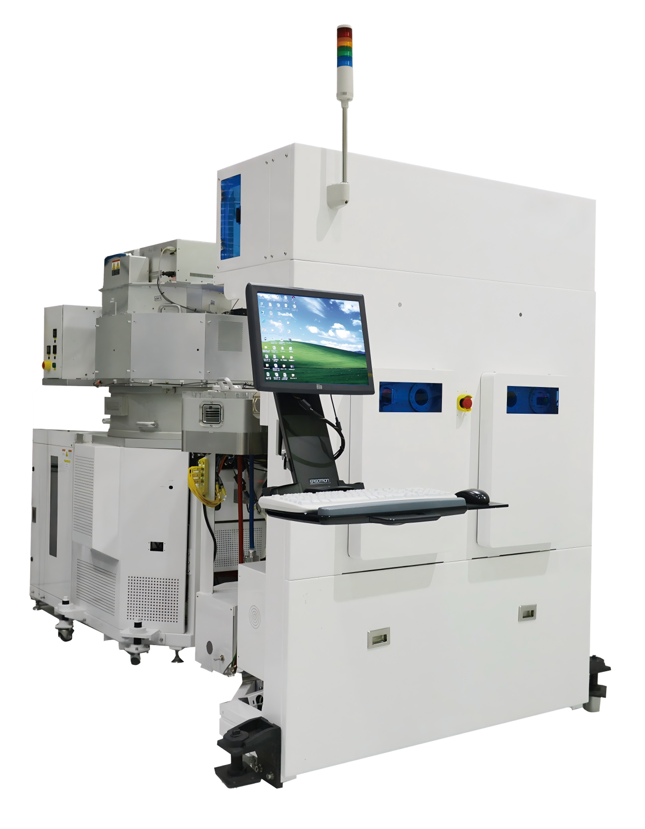
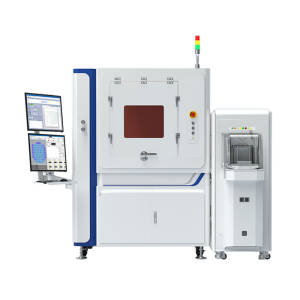
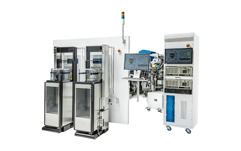
Testing is the core quality control barrier to screen qualified chips and eliminate defective products. TheWafer Test SystemĀ conducts comprehensive electrical performance detection on uncut wafer dies before packaging, verifying circuit conductivity, functional integrity and operational stability, and marking defective dies in advance to avoid invalid subsequent processing. After packaging, finished chips undergo secondary systematic testing covering functional verification, reliability inspection and environmental adaptability assessment. Only products that pass all strict test standards can enter the commercial supply chain, ensuring consistent and reliable performance of delivered chips.

5. Intelligent Supply System

The entire chip manufacturing process relies on a stable and intelligent supporting supply system, mainly supported by CDS and SDSĀ systems. These professional systems undertake core tasks such as clean environment monitoring, process gas and liquid supply, power stability control and production data scheduling. They maintain ultra-clean, constant-temperature and constant-humidity production conditions for processing equipment, ensure continuous and stable supply of all process materials, and realize real-time monitoring and intelligent management of the whole production flow. The supply system is the invisible guarantee for standardized, high-efficiency and low-defect chip mass production.

CDS and SDSĀ systems

Conclusions

From substrate cleaning and micro-nano fabrication to precision packaging, rigorous testing and systematic supply guarantee, every link of chip processing is highly collaborative and precision-oriented. The iteration and optimization of core equipment and supporting systems continue to drive the upgrading of semiconductor manufacturing technology, supporting the high-quality development of the global electronics industry.

Leave a Reply

Your email address will not be published. Required fields are marked *